
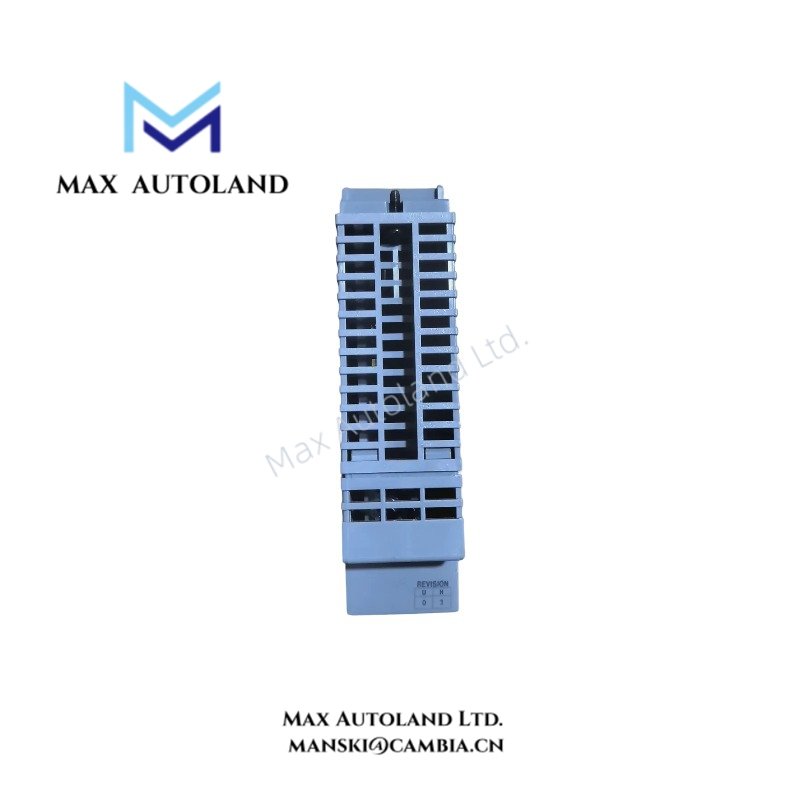
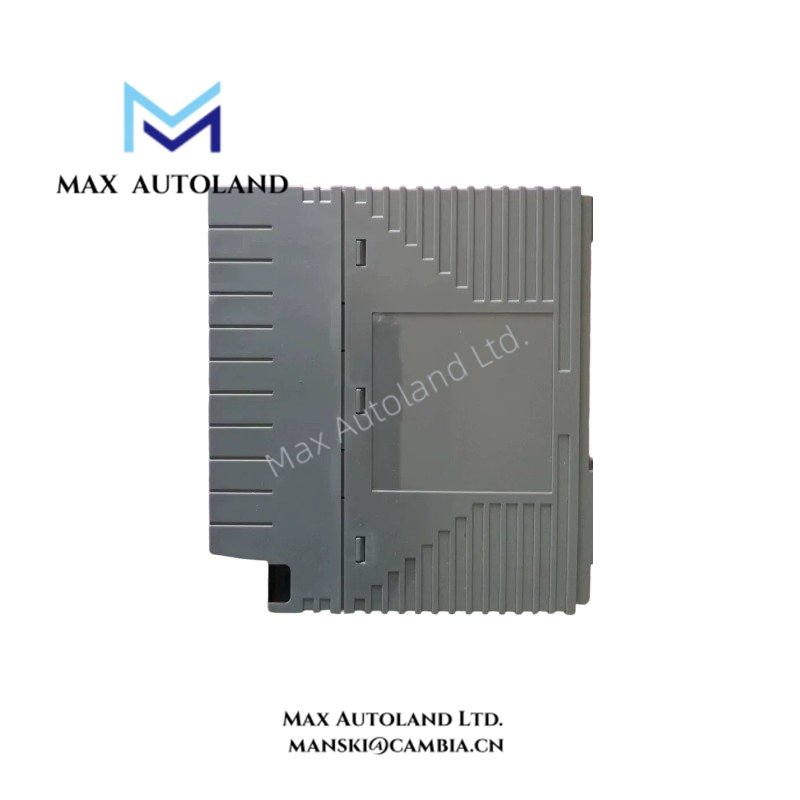
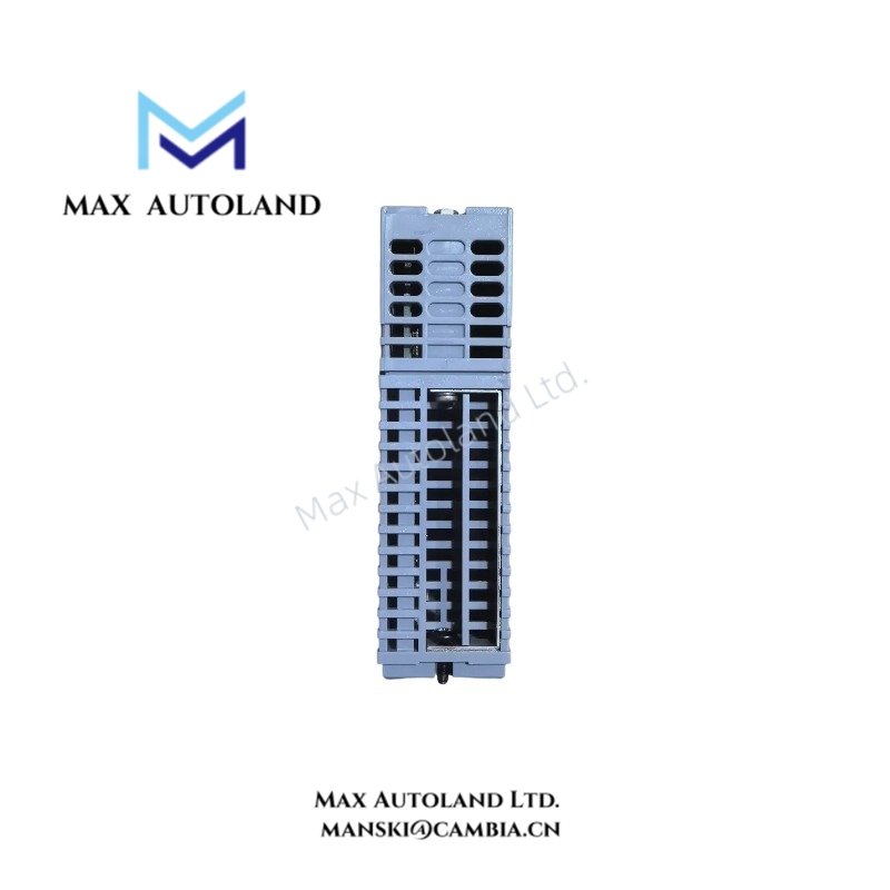
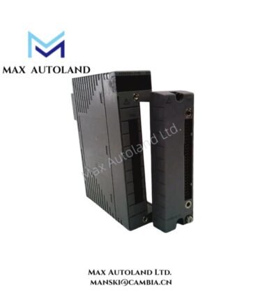
Overview
Technical Specifications
| Parameter | Specification |
|---|---|
| Model | ADV569-P01 |
| Brand | Yokogawa |
| Product Type | Digital Output Module |
| Module Family | Digital I/O Modules (CENTUM-ST Compatible) |
| Output Channels | 64 |
| Output Type | Transistor contact |
| Channel Isolation | Isolated |
| Common Configuration | Common minus side every 16 channels |
| Maximum Load Rating | 30 VDC, 100 mA |
| Load Types | Inductive and resistive loads |
| Output Response Time | 16 ms or less |
| Pulse Width / Time-Proportional Output Setting | 8 ms to 7200 s |
| ON Delay Time | 8 ms |
| OFF Delay Time | Add a maximum of 1 ms to the ON delay time |
| Current Consumption | 800 mA at 5 VDC |
| Approximate Weight | 0.30 kg |
| Connection | Dedicated KS9 cable |
| Compatible Module Standard | ST7 compatible |
Output Functions and Signal Configuration
The ADV569-P01 uses transistor outputs to switch discrete field signals. Its 64 output channels support multiple control points within one module, while the common-minus configuration groups the channels in sets of 16. This arrangement must be considered when checking field wiring and signal grouping.
The module also supports pulse-width and time-proportional output functions. The specified setting range is 8 ms to 7200 s, allowing timed output patterns to be configured according to the control requirements.
Load and Timing Requirements
The specified maximum load rating is 30 VDC at 100 mA for inductive and resistive loads. Check the field device’s voltage and current requirements against these limits before selecting the module. Inductive loads may also require suitable suppression based on the connected device and circuit design.
The output response time is 16 ms or less. The specified ON delay is 8 ms, with an additional maximum of 1 ms for the OFF delay. These timing values should be considered when coordinating output signals with the response requirements of the controlled equipment.
Ordering Information
The supplied model and suffix information identifies the following configurations:
| Code | Description |
|---|---|
| ADV569 | Digital Output Module for compatible ST7 |
| -P | With pulse-width function / time-proportional output function |
| 0 | Fixed code |
| 0 | Basic type |
| 1 | With ISA Standard G3 option |
The documented ordering variants are ADV569-P00 and ADV569-P01. The P01 version includes the ISA Standard G3 option according to the supplied suffix definitions. Confirm the complete model code on the module nameplate before ordering a replacement.
Installation and Compatibility
The source specification lists the module for installation in the following units:
- ESB Bus Node Units: ANB10S, ANB10D
- Optical ESB Bus Node Units: ANB11S, ANB11D
- Field Control Units: AFV30S, AFV30D, AFV40S, AFV40D
The specification also identifies the module as ST7 compatible. Verify the installed system configuration and the required KS9 dedicated cable before replacement or commissioning.
Frequently Asked Questions
Q: How many output channels does the ADV569-P01 provide?
A: It provides 64 transistor output channels, with a common-minus connection shared by each group of 16 channels.
Q: What are the maximum output load ratings?
A: The specified load rating is 30 VDC and 100 mA for inductive and resistive loads. The connected field device must remain within these limits.
Q: What is the difference between ADV569-P00 and ADV569-P01?
A: The supplied suffix definitions identify P01 as the version with the ISA Standard G3 option, while P00 is the basic type. Verify the nameplate and ordering code when matching an existing installation.
YOKOGAWA Top Products
Customers Also Viewed




Reviews
There are no reviews yet.